Lesson 1. Binary Logic
Lesson Objective
- Construct truth tables for the following logic gates: NOT, AND, OR, XOR, NAND, NOR
- Be familiar with drawing and interpreting logic gate circuit diagrams involving one or more of the above gates.
- Complete a truth table for a given logic gate circuit.
- Write a Boolean expression for a given logic gate circuit.
- Draw an equivalent logic gate circuit for a given Boolean expression.
- Recognise and trace the logic of the circuits of a half-adder and a full-adder.
- Construct the circuit for a half-adder.
- Be familiar with the use of the edge-triggered D-type flip-flop as a memory unit.
- Knowledge of internal operation of this flip-flop is not required.
Lesson Notes
Binary Logic?
Electronic circuits that perform Binary functions are called logic gates. Logic Gates form the basis of all logic circuits.
- A high voltage represents one state, logic 1
- A low voltage represents the other state, logic 0
Logic Gates represent Boolean Equations. Each Boolean function is represented by a different symbol.
Truth Tables
A truth table shows the results of Boolean equation from all possible combinations of inputs. They are used to show all possible outcomes from Boolean equations and logic gate diagrams. The truth table and logic gate symbol for show on the right of the screen. Or below on mobile browsers.
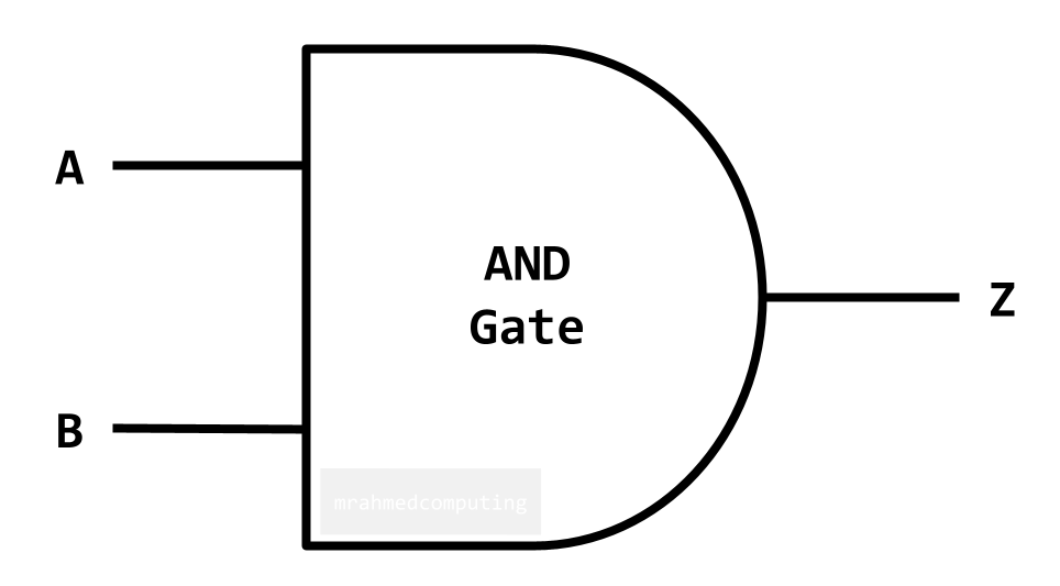
AND Gate
For an AND Gate the output is TRUE only if ALL inputs are TRUE.
Boolean Algebra Notation:
- Z = A ∧ B
- Z = A . B
- Z = A AND B
- Z = AB
| A |
B |
Z |
| 0 |
0 |
0 |
| 0 |
1 |
0 |
| 1 |
0 |
0 |
| 1 |
1 |
1 |
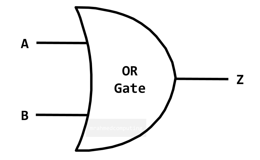
OR Gate
For an OR Gate the output is TRUE if EITHER/ALL inputs are TRUE.
Boolean Algebra Notation:
- Z = A ∨ B
- Z = A + B
- Z = A OR B
| A |
B |
Z |
| 0 |
0 |
0 |
| 0 |
1 |
1 |
| 1 |
0 |
1 |
| 1 |
1 |
1 |
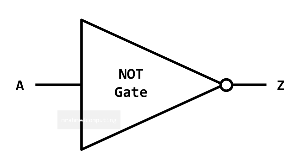
NOT Gate
For a NOT Gate the output is the OPPOSITE (inverse) of the input.
Boolean Algebra Notation:
- Z = ¬A
- Z = Ā
- Z = NOT(A)
- Z = A'
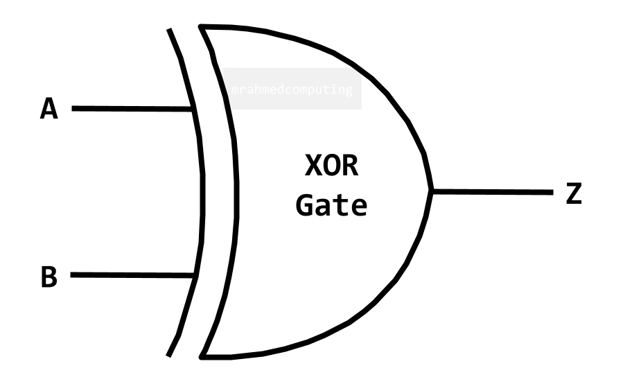
XOR Gate
For an XOR Gate the output is TRUE if only ONE input is TRUE.
Boolean Algebra Notation:
- Z = A ⊻ B
- Z = A ⊕ B
- Z = A XOR B
| A |
B |
Z |
| 0 |
0 |
0 |
| 0 |
1 |
1 |
| 1 |
0 |
1 |
| 1 |
1 |
0 |
NAND Gate
For an NAND Gate the output is TRUE if both input are NOT TRUE.
Boolean Algebra Notation:
- Z = A ? B
- Z = A ? B
- Z = A NAND B
| A |
B |
Z |
| 0 |
0 |
1 |
| 0 |
1 |
1 |
| 1 |
0 |
1 |
| 1 |
1 |
0 |
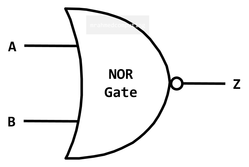
NOR Gate
For an NOR Gate the output is TRUE if EITHER/BOTH of the inputs are NOT TRUE.
Boolean Algebra Notation:
- Z = A ? B
- Z = A ? B
- Z = A NOR B
| A |
B |
Z |
| 0 |
0 |
1 |
| 0 |
1 |
0 |
| 1 |
0 |
0 |
| 1 |
1 |
0 |
Logic Circuits
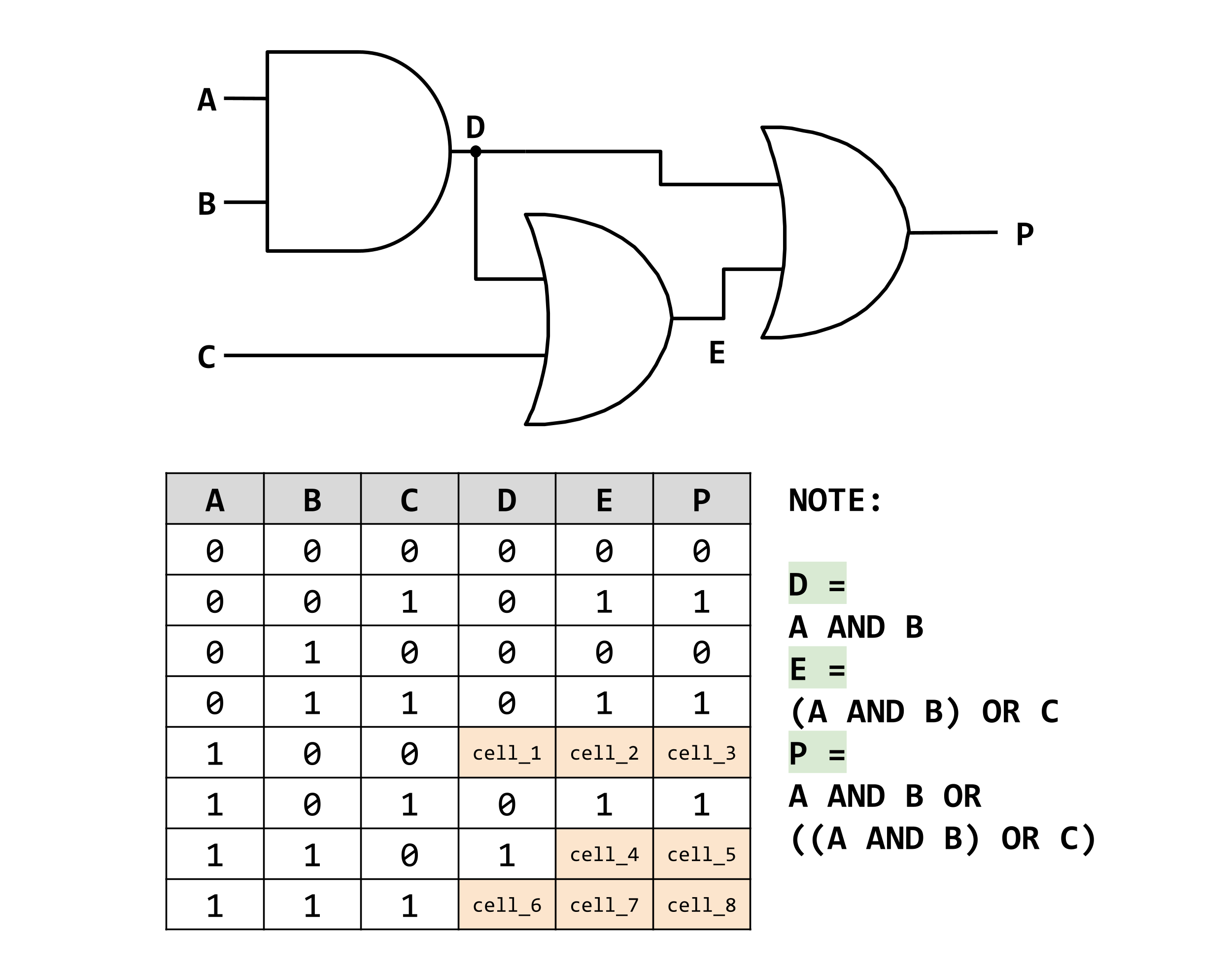
Identifing Expressions and Complteting a Truth Table
The output expressions have been labelled and noted in the diagram.
- Cell 1 is the result of A(1) and B(0) going into an AND gate. As both inputs are not TRUE the output (Cell_1) will be FALSE(0).
- Cell 2 is the result of D(0) and C(0) going into an OR gate. As both inputs are FALSE so the output (Cell_2) will be FALSE(0).
- Cell 3 is the result of D(0) and E(0) going into an OR gate. As both inputs are FALSE so the output (Cell_3) will be FALSE(0).
Can you work out the outputs for the remaining cells?
Adders
Electronic circuits called adders are used to add together binary numbers. Adders are formed by combining logic gates together. Adders are found inside the ALU of the CPU. There are two main types, the half and the full adder.
Half Adders
A half adder circuit is used to take a 2 bit binary input and produce a 2 bit binary output which is correct to the rules and result of a binary addition.
Rules of Addition
- 0 + 0 = 0
- 0 + 1 = 1
- 1 + 0 = 1
- 1 + 1 = 0 Carry 1
The half-adder has only two inputs so it cannot use the carry from a previous addition as a third input to a subsequent addition. It can only add one-bit numbers.
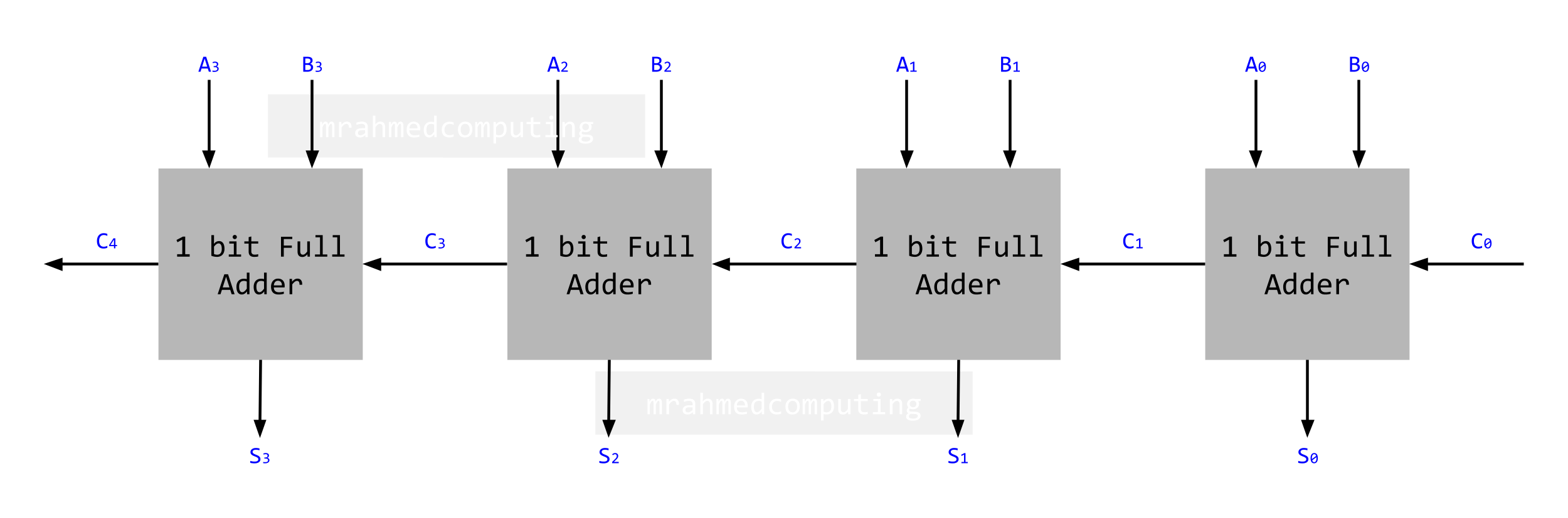
Full Adders
A full adder combines two half adders, with an extra OR gate. Now we can add a 3-bit input to include the inputs A and B along with the carry bit.
Concatenating Full Adders
Multiple full adders can be connected together. n full adders can be connected together to input the carry bit into a subsequent adder along with two new inputs.

The concatenated adder can now add two binary numbers each of n bits.
D-Type Flip Flop
A flip flop is an elemental sequential logic circuit that can store one bit and flip between two states, 0 and 1. A D-type flip flop has two inputs D (data) and a Clock signal, and two outputs Q and NOT Q.
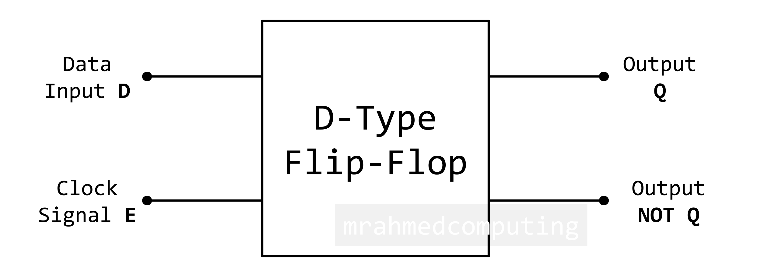
D-Type Flip Flop - Clock
The clock (or oscillator) is another type of sequential circuit that changes state at regular time intervals. It is needed to synchronise the change of state of flip flop circuits.

An edge-triggered D-type flip-flop only changes on the rising edge of the clock signal.
D-Type Flip Flop - Memory
Output Q only takes on a new value if the value at D has changed at the point of a clock pulse.
This means that the clock pulse will freeze or ‘store’ the input value at D, in Q until the next clock pulse.
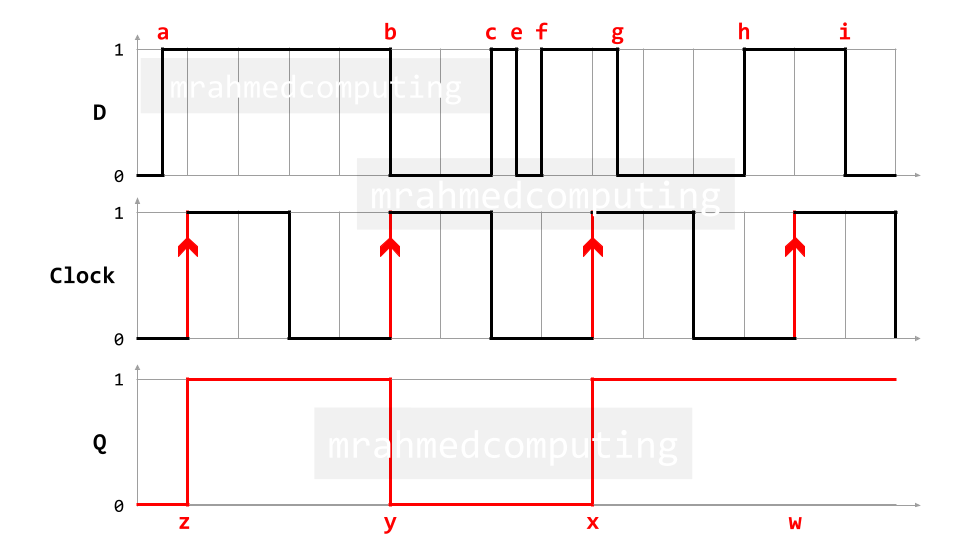
In the example above, D changes at times (rising edge of clock) marked a,b,c,e,f,g,h,i.
If D is the same on the next clock pulse, the flip flop will retain its current value, otherwise it will flip.
Output Q changes at times marked z,y,x,w.
D-type flip-flops are used for creating registers and counters. It is important because it can be used as a memory cell to store that state of a bit. Effectively, it is 1-bit memory.
To store 8-bits, 8 flip flops are needed. They are used for the intermediate storage needed during arithmetic operations.